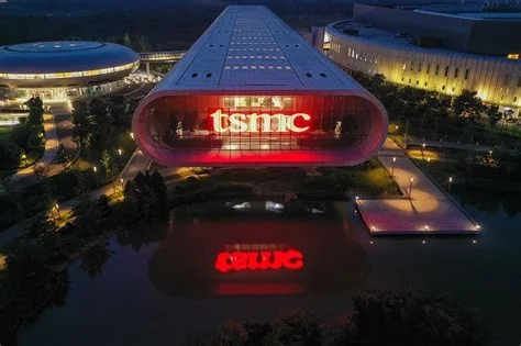
TSMC is set to start mass production of 3‑nanometre AI chips at its new Kumamoto fab, marking the first advanced‑node facility on Japanese soil. The plant targets soaring AI, robotics and autonomous‑driving workloads, and it gives you a faster path to cutting‑edge silicon while strengthening Japan’s chip sovereignty and promises quicker time‑to‑market for local designers.
Why the Kumamoto 3nm Fab Matters
The 3nm node delivers higher transistor density, lower power draw, and superior performance—key traits for training large language models, running edge inference, and powering next‑generation autonomous vehicles. By locating this capability in Japan, TSMC helps you reduce latency and diversify supply chains, which is crucial amid rising geopolitical tensions.
Boosting Japan’s Semiconductor Strategy
Hosting a 3nm fab narrows the gap between Japan and other semiconductor powerhouses. The government’s backing turns the plant into a strategic anchor, insulating critical AI workloads from external shocks and encouraging local talent to specialize in ultra‑advanced lithography.
TSMC’s Global Fab Cluster
Beyond Kumamoto, TSMC is expanding its Arizona facilities, creating a tri‑regional network that serves global customers with minimal latency. This cluster approach lets you tap into a seamless production flow from the United States to Japan, enhancing flexibility for high‑performance designs.
What the New Chips Enable
- AI acceleration: Faster training cycles and more efficient inference at the edge.
- Robotics: Higher precision control with reduced power consumption.
- Autonomous driving: Real‑time processing that meets safety‑critical demands.
Industry Implications
The investment signals that the AI boom isn’t a passing hype; major foundries are committing billions to meet real demand. Competitors will feel pressure to accelerate their own roadmaps, and the added geographic node reshapes logistics, talent flows, and export‑control considerations.
Perspective for Design Engineers
For you, the message is clear: upcoming products will be built around 3nm capabilities. Access to a Japanese production line could shave weeks off time‑to‑market, especially if your supply chain already spans the region.
Job Opportunities in Kumamoto
Even while construction continues, the hiring drive is in full swing. Skilled technicians, process engineers, and equipment specialists are being recruited to staff the high‑precision environment required for 3nm lithography. This surge promises to cultivate a new generation of semiconductor experts right in Japan.
Looking Ahead
With a $17 billion investment and strong political support, the Kumamoto plant positions TSMC at the heart of the AI future. Whether the venture meets its lofty expectations will depend on how quickly AI workloads translate into sustained wafer orders, but one thing’s certain: the new fab is a pivotal piece in the global race for advanced silicon.