Neurophos, an Austin‑based photonic computing startup, closed a $110 million Series A round to accelerate development of its exaflop‑scale photonic AI accelerator. The funding will fund chip production, a full software stack, and new engineering sites, positioning the company to deliver a drop‑in GPU replacement that promises up to 100× higher performance‑per‑watt for data‑center workloads.
Series A Funding Details and Strategic Investors
The $110 million round was led by Gates Frontier and included participation from Microsoft’s venture fund M12, Carbon Direct Capital, Aramco Ventures, Bosch Ventures, Tectonic Ventures, Space Capital, and other investors. The capital brings Neurophos’s total funding to $118 million and is earmarked for rapid development, commercial launch, and expansion of its Austin headquarters and a new engineering site in San Francisco.
Technology Overview: Exaflop‑Scale Photonic AI Accelerator
Optical Processing Unit Architecture
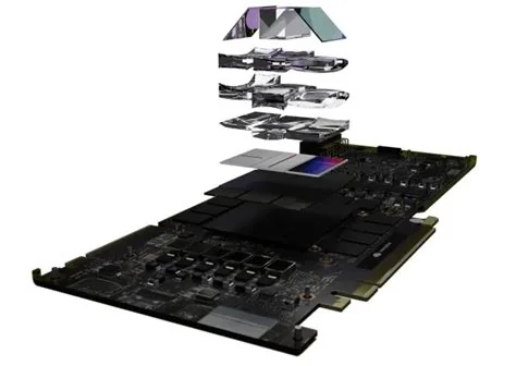
At the core of Neurophos’s chip is a proprietary Optical Processing Unit (OPU) that integrates more than one million micron‑scale optical processing elements on a single silicon substrate. A breakthrough in metamaterial optical modulators—10,000 × smaller than previous photonic components—enables this unprecedented density, making large‑scale, manufacturable photonic computing feasible for the first time.
Performance and Energy Efficiency Claims
Neurophos describes the accelerator as a “drop‑in replacement for GPUs” that delivers up to 100 × the performance‑per‑watt of today’s leading silicon chips. With exaflop‑scale throughput—one quintillion floating‑point operations per second—the OPU is designed to handle the most demanding AI inference and training workloads while dramatically reducing power consumption and thermal load.
Market Impact and Competitive Landscape
The AI compute market has long been dominated by silicon‑based GPUs and custom ASICs such as Google’s TPU. As model sizes continue to grow, power and thermal budgets of conventional data‑center hardware are being stretched to their limits. Photonic computing leverages light instead of electrons, offering orders‑of‑magnitude improvements in bandwidth and energy efficiency. Neurophos’s achievement of a million‑element OPU on a single chip represents a significant engineering milestone that could reshape the economics of AI inference and training.
Roadmap and Future Plans
Series A proceeds will fund the accelerated delivery of Neurophos’s first integrated photonic computing system, including early‑access hardware for developers and a complete software ecosystem. The company aims for a near‑term datacenter launch, followed by broader ecosystem integration. Expansion of its Austin headquarters and the new San Francisco engineering site will support hardware development, software stack creation, and early‑access programs for developers.
Implications for AI Infrastructure
If the performance and efficiency targets are met, Neurophos’s photonic AI chip could lower operating costs for hyperscale cloud providers and enterprises deploying large language models. The “drop‑in” nature of the accelerator may reduce adoption friction, allowing existing software stacks to leverage photonic performance gains without extensive redesign. Strategic investment from major cloud and AI players underscores the growing interest in photonic solutions as a pathway to extend the lifespan of compute infrastructure.


