Samsung Electronics has begun mass‑producing its sixth‑generation high‑bandwidth memory, HBM4, and will start shipping the chips to Nvidia within weeks. The new memory delivers up to 3 TB/s per stack, giving AI accelerators a sizable bandwidth boost while Samsung secures a three‑month lead over rivals. This early launch positions Samsung as the primary supplier for next‑gen AI hardware and signals a shift in the competitive landscape.
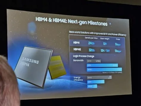
HBM4 Performance Gains Over HBM3E
HBM4 pushes data rates to 11.7 Gbps per pin, a 22 % jump from HBM3E and roughly 37 % above the JEDEC baseline. In real‑world terms, each stack can move up to 3 TB/s of data, delivering about 2.4 times the throughput of the previous generation. Those numbers translate into faster model training and inference for the massive transformer networks that dominate AI workloads today.
Integrated Manufacturing Gives Samsung an Edge
Samsung fabricates the logic die on its own 4‑nm line and couples it with a 10‑nm‑class 1‑c DRAM stack, all within the same Plant 4 facility. This vertically integrated process lets the company meet Nvidia’s strict quality and power‑efficiency targets, earning top scores in final verification tests.
Market Impact and Timing Advantage
While SK Hynix has pushed its HBM4 mass‑production timeline to March‑April, Samsung’s chips are already shipping, giving it a three‑month head start. Micron plans to ramp up output in the second quarter of next year, leaving Samsung firmly ahead. The market reacted quickly: Samsung’s shares jumped between 4.9 % and 6.4 %, and Nvidia’s stock rose 7.87 % on the news.
Implications for AI Chipmakers
Analysts have warned that AI vendors need a three‑supplier memory strategy to avoid single‑source risk. With Samsung delivering high‑performance, high‑capacity HBM4 on schedule, Nvidia can diversify away from its historic reliance on SK Hynix. The added bandwidth also helps keep the power envelope in check—a crucial factor for data‑center operators who pay for every watt.
Future Capacity Expansion Plans
Samsung aims to boost its HBM output by about 50 % by the end of the year, targeting roughly 250,000 wafers per month—up from the current 170,000. A new DRAM line at Plant 4 will add another 100,000‑120,000 wafers monthly, raising overall DRAM output by 18 %.
What System Designers Say
“From a system‑design standpoint, the jump to 3 TB/s per stack simplifies board layout and reduces the number of memory channels we need to achieve petaflop‑scale performance,” says a senior memory architect who works with AI accelerator vendors. “The integrated 4‑nm logic‑on‑die also means lower latency between the GPU and memory, which can shave milliseconds off training loops—a tangible win for large‑scale models.”
What This Means for You
If you’re evaluating AI hardware for your data center, you’ll want to factor in Samsung’s HBM4 bandwidth and its early‑bird availability. The faster memory can lower training times, reduce power costs, and give you more flexibility in supplier choices. Keep an eye on Samsung’s capacity expansion—its success could make it the go‑to memory partner for the next generation of AI systems.