Intel is teaming up with TSMC to tap its cutting‑edge 2‑nm wafer lines and advanced packaging services, aiming to get AI accelerators into U.S. data centers faster. By combining Intel’s 18A silicon with TSMC’s high‑density interposers, the partnership promises higher bandwidth, lower latency, and a more resilient domestic supply chain for your AI workloads.
Why Advanced Packaging Matters for AI
Modern AI models demand massive data movement between compute cores and memory. Simply shrinking transistors isn’t enough; you need to stack high‑bandwidth memory (HBM) close to the processor to keep power draw low and latency short. That’s why packaging has become the bottleneck that determines how quickly you can scale AI workloads.
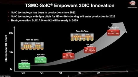
TSMC’s Packaging Technologies
CoWoS and InFO Explained
TSMC’s CoWoS (Chip‑on‑Wafer‑on‑Substrate) and InFO (Integrated Fan‑Out) technologies let manufacturers place HBM dies directly on top of a processor. The result is a nanosecond‑level reduction in data travel time and a dramatic boost in bandwidth per square millimeter. Engineers rely on these flows because they deliver high yield while maintaining tight thermal budgets.
Intel’s Strategic Use of TSMC’s 2‑nm Fab
Intel will source wafers from TSMC’s 2‑nm (N2) production lines in Taiwan while planning to use TSMC’s upcoming U.S. packaging footprint. This approach gives Intel immediate access to the most advanced node without waiting for its own fab upgrades, and it shortens the time‑to‑market for AI accelerators that your organization needs.
Impact on the U.S. AI Ecosystem
U.S. cloud providers, enterprise AI teams, and defense contractors all benefit from a domestic packaging option. By reducing reliance on overseas fabs, the collaboration eases geopolitical risk and helps close the HBM shortage that has been throttling AI model growth. You’ll see faster delivery times and more predictable pricing as the two giants align their roadmaps.
- Higher bandwidth: More HBM lanes per millimeter improve data throughput.
- Lower latency: Stacked memory cuts the distance between compute and storage.
- Domestic resilience: U.S.-based packaging mitigates supply‑chain disruptions.
- Faster time‑to‑market: Leveraging TSMC’s mature processes accelerates product launches.
What Engineers Are Saying
Packaging engineers on the floor describe the partnership as a logical step toward “design‑for‑package” thinking. When silicon nodes align with a proven, high‑yield packaging platform, lead times shrink dramatically and the risk of yield loss at the package level drops. Combining Intel’s PowerVia backside‑power delivery with TSMC’s dense interposers could let AI accelerators hit both performance and power targets without the usual trade‑offs.
In short, Intel’s alignment with TSMC isn’t a headline‑grabbing merger; it’s a strategic move that acknowledges where the real AI‑chip advantage lives today—advanced, high‑bandwidth packaging. If the two companies keep their roadmaps in sync, the U.S. AI market will finally get the supply‑chain resilience it’s been craving.